PCB PROFESSIONAL MANUFACTRRER!
PCB PROFESSIONAL MANUFACTRRER!

Ensuring the highest standards in packaging quality control is essential to protect products during transit and maintain brand integrity. Our process involves rigorous inspections at every stage of packaging, from material selection to final sealing. We verify that packaging materials meet specified strength and durability requirements and conduct tests for proper sealing, weight distribution, and resistance to environmental factors. Our team is trained to identify and rectify any defects, ensuring that every package meets our strict quality criteria before it reaches the customer.
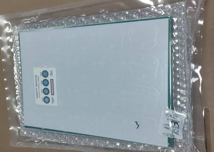
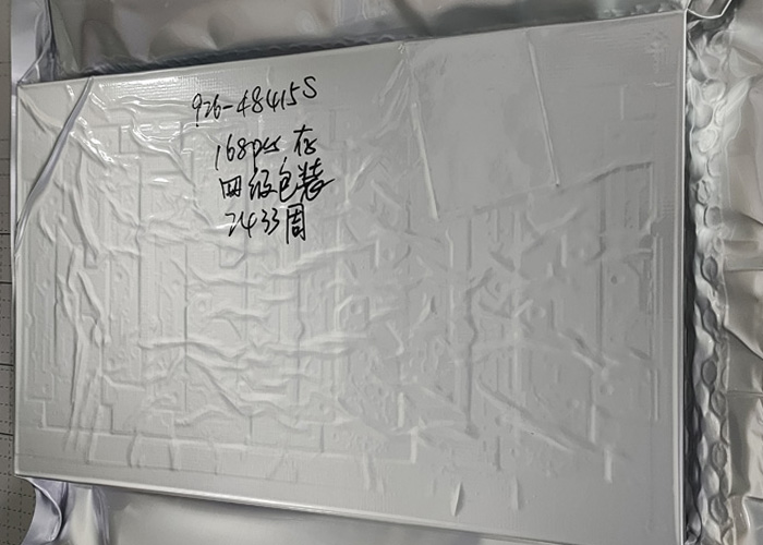
To further guarantee packaging quality, our company offers three different types of packaging materials: bubble film, PE bags, and aluminum foil. Below are examples of each type of packaging."
customer can choose any style package what they want
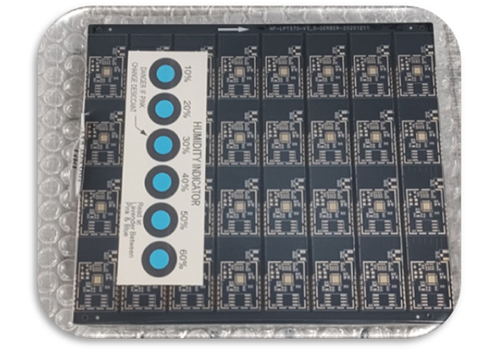
Bubble film packaging is a universal packaging in the circuit board industry. We will put moisture-proof agent in the packaging. Some customers require humidity card in addition . To be honest, this kind of packaging cannot have higher moisture-proof function like PE BAG or aluminum foil bag, so it is meaningless to put humidity card.
Dual-Use Packaging for PCB Boards.In the PCB industry, dual-use packaging offers versatile protection and convenience for handling and shipping circuit boards. This innovative packaging solution is designed to serve both protective and functional purposes, ensuring that PCBs are securely protected during transit while also being easy to handle and store.
Additionally, dual-use packaging is engineered for efficiency, allowing for easy stacking and storage. This reduces the overall footprint and simplifies inventory management. By combining protective qualities with practical handling features, our dual-use packaging ensures that PCB boards arrive in optimal condition, meeting the highest standards of quality and reliability.
But its cost is a little bit high than the bubble film package.
Dual-Use Packaging for PCB Boards.In the PCB industry, dual-use packaging offers versatile protection and convenience for handling and shipping circuit boards. This innovative packaging solution is designed to serve both protective and functional purposes, ensuring that PCBs are securely protected during transit while also being easy to handle and store.
Additionally, dual-use packaging is engineered for efficiency, allowing for easy stacking and storage. This reduces the overall footprint and simplifies inventory management. By combining protective qualities with practical handling features, our dual-use packaging ensures that PCB boards arrive in optimal condition, meeting the highest standards of quality and reliability.
Aluminum foil bags combined with bubble film represent the most costly packaging option among the three available styles. This high cost reflects the superior level of protection they offer, including enhanced moisture resistance and impact cushioning, compared to other packaging methods."
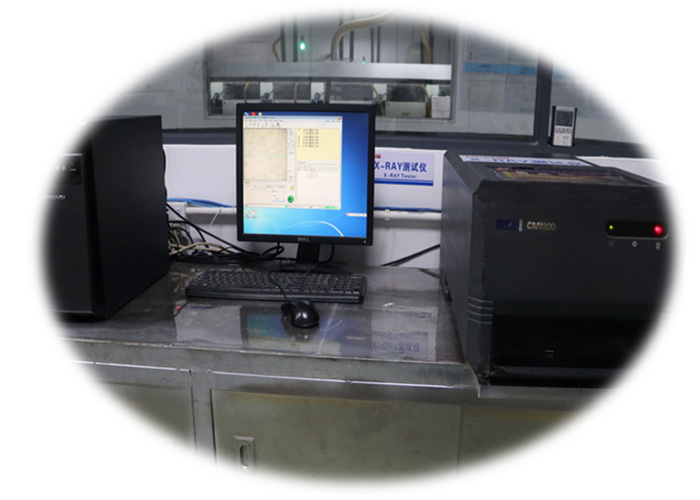
To guarantee that the thickness of surface coatings on our PCB boards meets customer specifications, our company has invested in an advanced X-RAY detector. This technology allows us to accurately measure the thickness of critical surface coatings, including gold, nickel, and tin.
By testing the thickness of these coatings, we ensure that each PCB board adheres to the required standards, preventing issues such as insufficient or excessive coating that could affect conductivity, solderability, or long-term reliability.
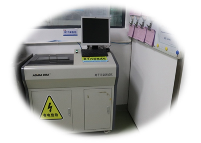
To meet the high-quality requirements of our customers, particularly regarding solderability, our company has invested in an advanced ion contamination tester. This equipment is essential for ensuring that all PCB boards we ship are clean and free from any foreign matter residues that could compromise solderability.
By identifying and eliminating ion contamination, we prevent potential solderability problems that could arise during assembly. This proactive approach reduces the risk of defects, minimizes rework, and ensures that the final product meets the customer's expectations.
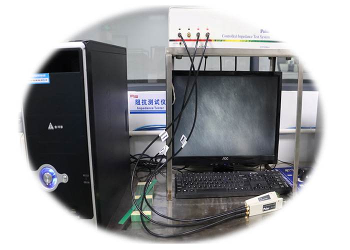
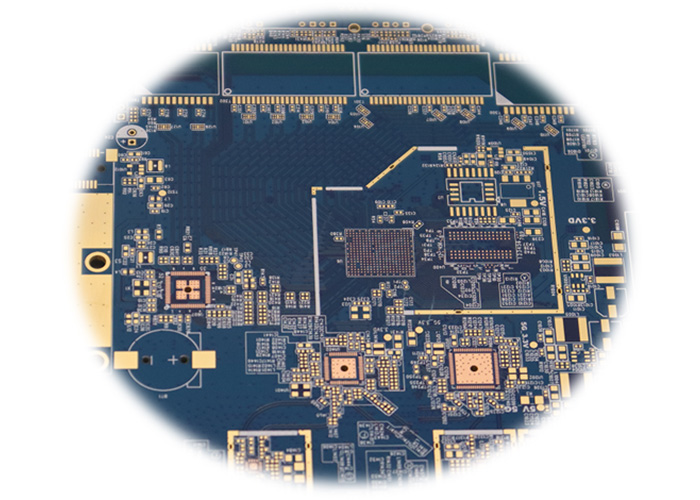
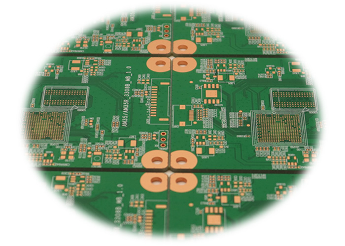
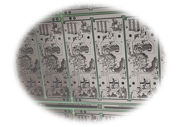
Specializing in the production of characteristic impedance PCB boards, our company excels in manufacturing multi-layer boards that meet various impedance requirements. Customers often specify different impedance values, such as 50 ohm, 80 ohm, and 100 ohm etc, across different conductor areas in their product designs. These requirements are well within our capabilities. With advanced impedance testing equipment, we ensure comprehensive quality control from design through to manufacturing, guaranteeing that our boards meet the exact specifications needed."
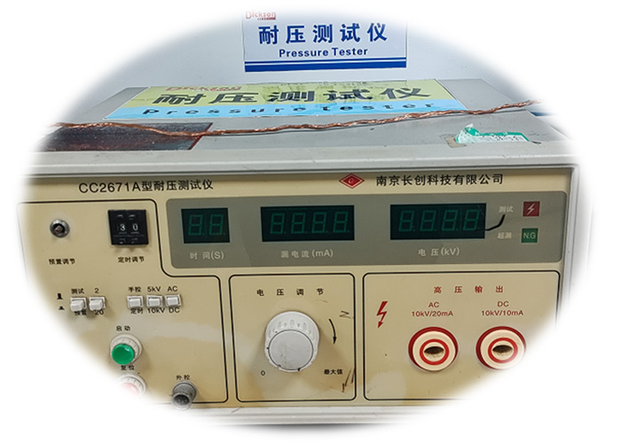
Our company utilizes Hi-Pot testers primarily for power supply PCBs with thick copper plating, which are integral to industrial power supply products used by our customers. To ensure the highest standards of product quality, we have invested in advanced high voltage testing equipment. This allows us to rigorously assess the PCB's ability to withstand specified voltage and current parameters, ensuring that every board we deliver fully meets our customers' stringent requirements."
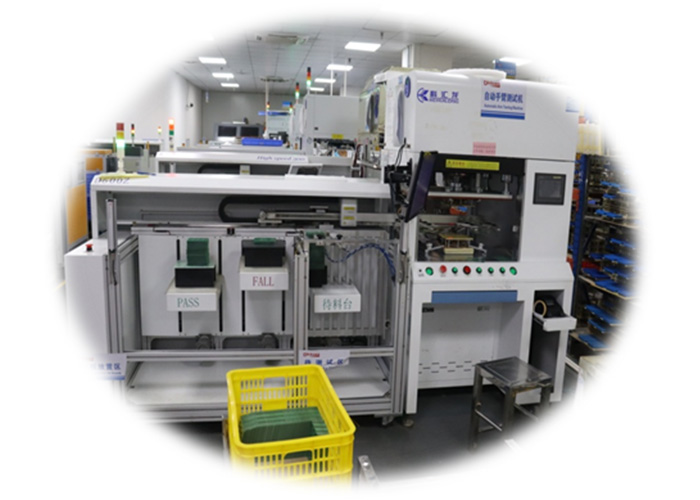
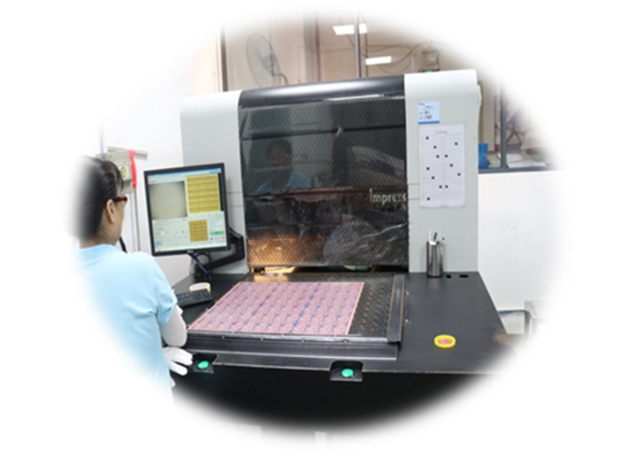
To guarantee product quality and prevent defective items from reaching the customer market, we have implemented a state-of-the-art automatic testing machine for electrical function testing. This advanced equipment plays a crucial role in our quality control process by rigorously evaluating the electrical integrity of each PCB board before it is shipped.
We conduct a 100% electrical function test on all bare PCB boards before shipment to ensure that no faulty PCBs are sent to our customers..
The automatic testing machine performs thorough electrical function tests, ensuring that each PCB board meets the required specifications and operates as intended. By detecting issues such as shorts, opens, or incorrect connections, the machine helps us identify and eliminate defective products before they reach the customer.
The use of automated testing minimizes the risk of human error, ensuring consistent and accurate results for every board tested. This reliability is crucial for maintaining the high standards that our customers expect and trust.
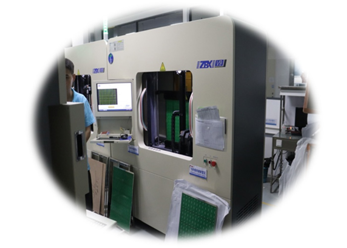
Customer orders often vary greatly in terms of product type and quantity, particularly during the initial stages of product development when order volumes are typically small. To better serve our customers and adapt to these varying demands, we have invested in a lot of flying probe testers.
Unlike traditional testing methods that require custom test fixtures, flying probe testing eliminates the need for these fixtures. This means that customers can avoid the high initial costs associated with fixture development, making it an ideal solution for small-quantity orders and prototypes.
We conduct a 100% electrical function test by flying probe test for all small quantity order's PCB board before shipment to ensure that no faulty PCBs are sent to our customers..
For customers in the early stages of product development, ensuring that their prototypes meet performance standards is crucial. Flying probe testing offers a reliable method for verifying the electrical functionality of these early-stage products, providing customers with the confidence they need before moving to larger-scale production.
We always committed to our customer,and offer our customers a cost-effective, flexible, and reliable testing solution. This not only reduces initial costs but also ensures that all products.
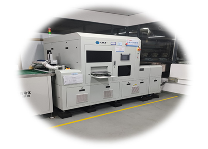
To uphold the highest standards of product quality, our company has made a substantial investment in Automated Optical Inspection (AOI) equipment. AOI technology is critical in the PCB manufacturing process, as it provides precise and consistent monitoring of each board at various stages of production, ensuring that every detail meets our strict quality criteria.
The developing stage in PCB manufacturing is critical because it is during this process that the circuit pattern on the board is formed. Accurate scanning and inspection of the board at this stage are essential to ensure that the integrity of the circuit pattern is maintained and that no defects are carried forward into subsequent processes.
To prevent these issues, an AOI inspection is performed immediately after the developing stage. AOI systems use high-resolution cameras and advanced algorithms to scan the entire surface of the PCB. They meticulously compare the actual circuit pattern against the intended design specifications, identifying even the smallest discrepancies or defects.
To prevent these issues, an AOI inspection is performed immediately after the developing stage. AOI systems use high-resolution cameras and advanced algorithms to scan the entire surface of the PCB. They meticulously compare the actual circuit pattern against the intended design specifications, identifying even the smallest discrepancies or defects.
AOI (Automated Optical Inspection) plays a vital role in ensuring the quality and reliability of PCB boards, particularly after the etching process. The etching stage is where the circuit pattern is fully realized, making it a critical point in the manufacturing process.
AOI inspection at this stage allows for a thorough comparison between the actual etched circuit and the customer’s design specifications. The AOI system scans the entire surface of the PCB, using high-resolution cameras and sophisticated software to detect even the smallest discrepancies. This ensures that the circuit pattern aligns precisely with the design intent, meeting all technical requirements.
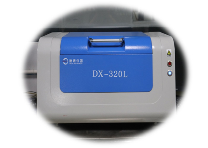
IQC (Incoming Quality Control) is crucial to maintaining our product quality. With the increasing demand for environmentally friendly products, many of our customers require that our PCB boards comply with ROHS standards. To prevent the introduction of non-compliant materials into our production process, we have invested in a ROHS detector. This enables us to rigorously test all incoming raw materials, ensuring that our PCB circuit board shipments fully meet ROHS requirements.
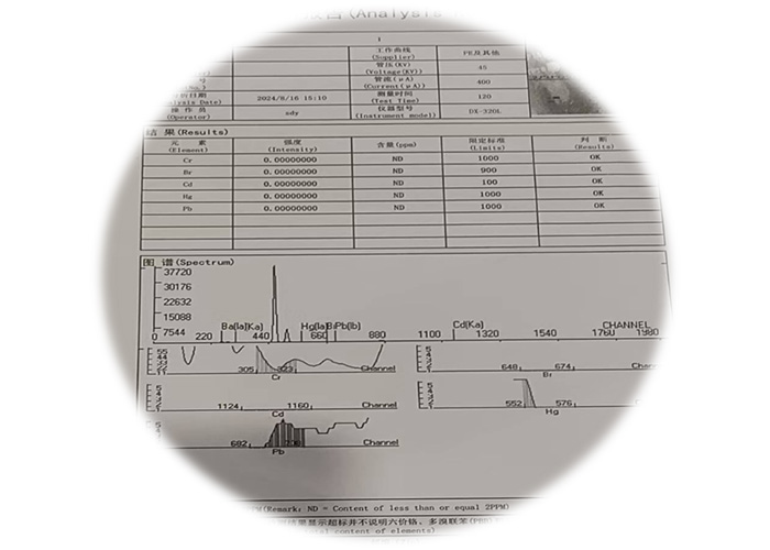
IQC plays a critical role in maintaining our product quality. As the demand for environmentally friendly products grows, many of our customers require that our PCB boards comply with ROHS standards. To ensure compliance, we perform ROHS testing on all externally sourced raw materials, including solder masks and laminates. By verifying that these materials meet ROHS standards, we ensure that the PCB boards we produce fully meet our customers' requirements.
Attached is a test result demonstrating compliance with ROHS standards
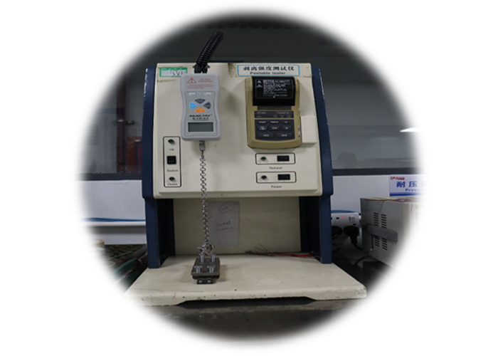
The copper foil tensile tester is a specialized piece of equipment used to evaluate the adhesion strength of copper on incoming PCB copper clad laminate materials. By testing these incoming laminates, we ensure the quality of the raw materials and, consequently, the adhesion quality of the copper foil in our finished PCB products. This rigorous testing process helps us meet and exceed our customers' product quality requirements."
"The copper foil tensile tester is a specialized device used to assess the adhesion strength of copper on incoming PCB copper clad laminate materials. We perform pull-strength tests on laminates of various thicknesses (e.g., 0.4mm, 0.6mm, 0.8mm, 1.0mm, 1.2mm, 1.6mm) and copper thicknesses (e.g., 0.5 oz, 1 oz, 2 oz, 3 oz) to ensure that all raw materials meet our quality standards. This rigorous testing ensures that the copper foil adhesion quality of our finished PCB products complies with our stringent requirements and those of our customers.
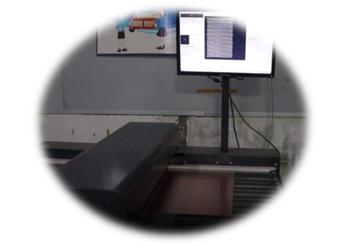
Our company bought a hole inspection machine to verify the number of holes on the PCB after the drilling process. This inspection ensures that the number of holes precisely aligns with the specifications provided in the customer's GERBER files, with no missing or extra holes, and no defects such as blocked holes.
The inspection machine uses optical technology, which offers greater reliability compared to manual visual inspections. Unlike human eyes, which are prone to fatigue and potential errors, the machine maintains consistent accuracy throughout the inspection process. This advanced approach guarantees that no holes are missed and significantly enhances the overall quality assurance of our PCBs.
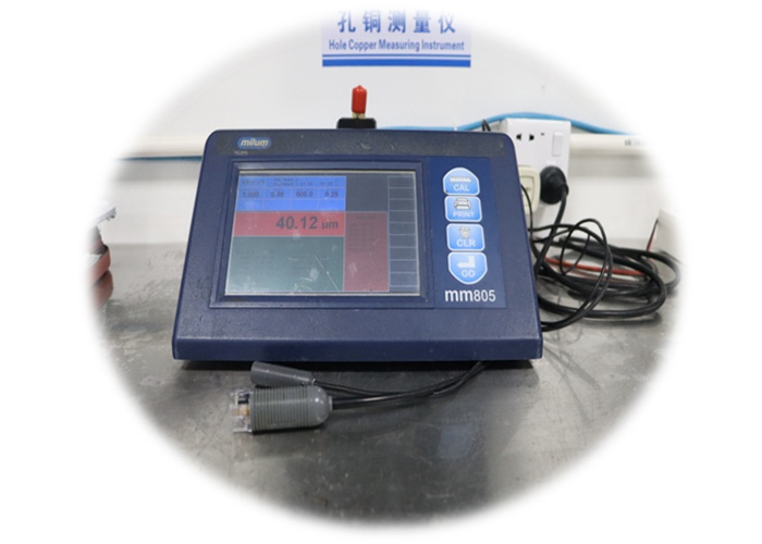
Electroplated Hole Quality Inspection
The quality of the electroplated hole diameter is critical to the overall quality of the circuit board, particularly regarding the thickness of the copper plating inside the hole. Insufficient copper thickness can negatively impact the lifespan of the PCB, while excessive thickness may interfere with the customer's plug-in assembly.
To ensure the accuracy of the hole diameter and copper thickness, our company has invested in a hole copper probe tester. This equipment allows for precise measurement of the copper plating thickness within the hole without damaging the PCB. By inserting the probe directly into the electroplated hole, we can quickly determine whether the copper thickness meets the specified requirements, thereby ensuring the product's quality aligns with customer expectations.
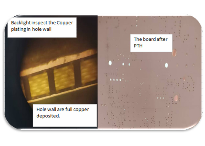
PTH Chemical Copper Quality Inspection
The quality of PTH (Plated Through Hole) chemical copper is crucial for the integrity of the PCB. If copper plating is insufficiently deposited during the PTH chemical copper stage, it can result in unplated areas within the holes, leading to voids and quality defects.
To ensure that the PTH chemical copper process is defect-free, we conduct backlight inspections for each PCB model during this stage. This inspection verifies that copper plating is uniformly deposited within the holes of the PCB, ensuring that the final hole copper quality meets the stringent requirements set by our customers
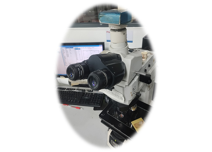
In our quality control process, we rigorously inspect all PCB boards before shipment to ensure they meet our stringent performance and reliability standards. This inspection involves a comprehensive microsection analysis performed on each board by using the special microscope . we assess the following critical parameters:
Hole Copper Thickness: We meticulously measure the thickness of the copper in hole wall. This ensures that the copper coating meets the specified requirements for electrical conductivity and mechanical strength, crucial for the performance and durability of the PCB.
Surface Copper Thickness: The thickness of the copper layer on the surface of the PCB is also evaluated. This measurement is essential to confirm that the surface copper meets the required standards.
Solder mask Layer Thickness: as solder mask is isolation protective layer to electrics product. which is applied to safeguard the copper and enhance the board's durability, is scrutinized. Ensuring the correct thickness of this layer is vital for maintaining the PCB’s reliability and resistance to environmental factors.
This meticulous inspection process is designed to guarantee that all products shipped from our facility meet or exceed customer specifications and industry standards, ensuring both performance and quality are upheld in every PCB delivered.

Tel.: +86 0755 2332 1191
Fax: +86 0755 8176 4499
Add.: Building A1, Zone B, Ditang Industrial Zone, Shasan Community Agricultural Company, Shajing Street, Bao'an District, Shenzhen
Copyright © DICKSON Circuit Shenzhen Co., Ltd. All Rights Reserved | Technical Support: Nbone


 sales@dspcb.com
 +86 13828761409
 CN
CN Home >