PCB PROFESSIONAL MANUFACTRRER!
PCB PROFESSIONAL MANUFACTRRER!

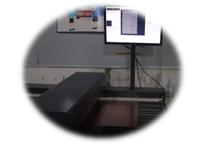
Our company bought a hole inspection machine to verify the number of holes on the PCB after the drilling process. This inspection ensures that the number of holes precisely aligns with the specifications provided in the customer's GERBER files, with no missing or extra holes, and no defects such as blocked holes.
The inspection machine uses optical technology, which offers greater reliability compared to manual visual inspections. Unlike human eyes, which are prone to fatigue and potential errors, the machine maintains consistent accuracy throughout the inspection process. This advanced approach guarantees that no holes are missed and significantly enhances the overall quality assurance of our PCBs.
Electroplated Hole Quality Inspection
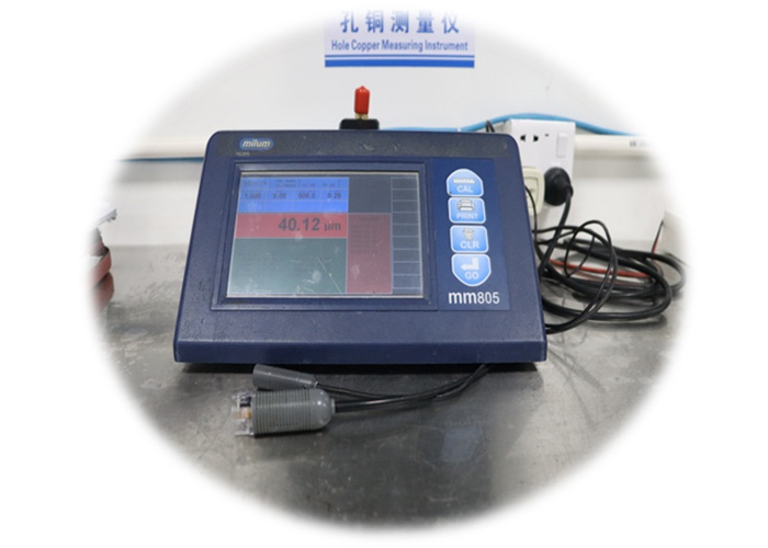
The quality of the electroplated hole diameter is critical to the overall quality of the circuit board, particularly regarding the thickness of the copper plating inside the hole. Insufficient copper thickness can negatively impact the lifespan of the PCB, while excessive thickness may interfere with the customer's plug-in assembly.
To ensure the accuracy of the hole diameter and copper thickness, our company has invested in a hole copper probe tester. This equipment allows for precise measurement of the copper plating thickness within the hole without damaging the PCB. By inserting the probe directly into the electroplated hole, we can quickly determine whether the copper thickness meets the specified requirements, thereby ensuring the product's quality aligns with customer expectations.
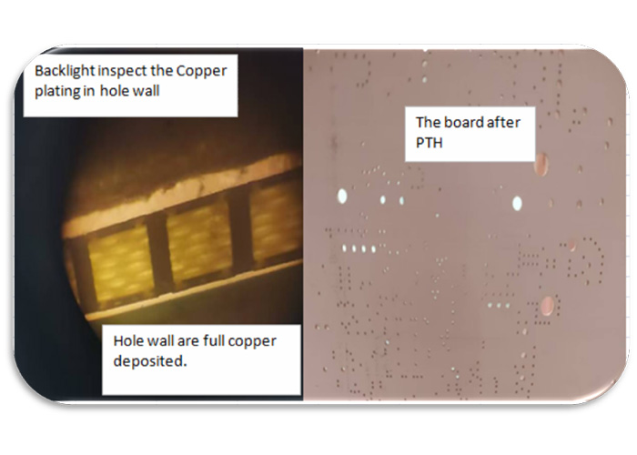
PTH Chemical Copper Quality Inspection
The quality of PTH (Plated Through Hole) chemical copper is crucial for the integrity of the PCB. If copper plating is insufficiently deposited during the PTH chemical copper stage, it can result in unplated areas within the holes, leading to voids and quality defects.
To ensure that the PTH chemical copper process is defect-free, we conduct backlight inspections for each PCB model during this stage. This inspection verifies that copper plating is uniformly deposited within the holes of the PCB, ensuring that the final hole copper quality meets the stringent requirements set by our customers
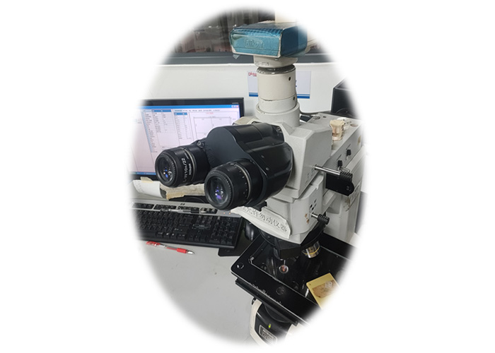
In our quality control process, we rigorously inspect all PCB boards before shipment to ensure they meet our stringent performance and reliability standards. This inspection involves a comprehensive microsection analysis performed on each board by using the special microscope . we assess the following critical parameters:
Hole Copper Thickness: We meticulously measure the thickness of the copper in hole wall. This ensures that the copper coating meets the specified requirements for electrical conductivity and mechanical strength, crucial for the performance and durability of the PCB.
Surface Copper Thickness: The thickness of the copper layer on the surface of the PCB is also evaluated. This measurement is essential to confirm that the surface copper meets the required standards.
Solder mask Layer Thickness: as solder mask is isolation protective layer to electrics product. which is applied to safeguard the copper and enhance the board's durability, is scrutinized. Ensuring the correct thickness of this layer is vital for maintaining the PCB’s reliability and resistance to environmental factors.
This meticulous inspection process is designed to guarantee that all products shipped from our facility meet or exceed customer specifications and industry standards, ensuring both performance and quality are upheld in every PCB delivered.

Tel.: +86 0755 2332 1191
Fax: +86 0755 8176 4499
Add.: Building A1, Zone B, Ditang Industrial Zone, Shasan Community Agricultural Company, Shajing Street, Bao'an District, Shenzhen
Copyright © DICKSON Circuit Shenzhen Co., Ltd. All Rights Reserved | Technical Support: Nbone


 sales@dspcb.com
 +86 13828761409
 CN
CN Home >