PCB PROFESSIONAL MANUFACTRRER!
PCB PROFESSIONAL MANUFACTRRER!

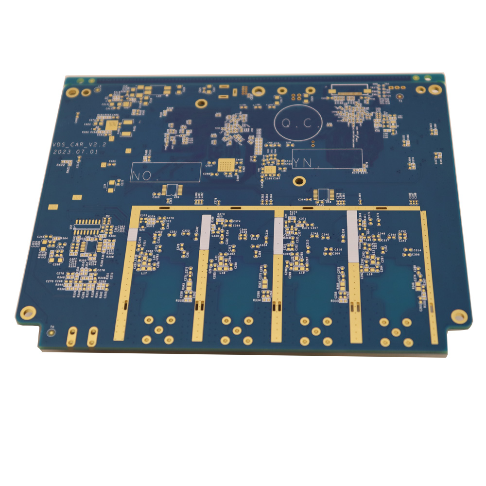
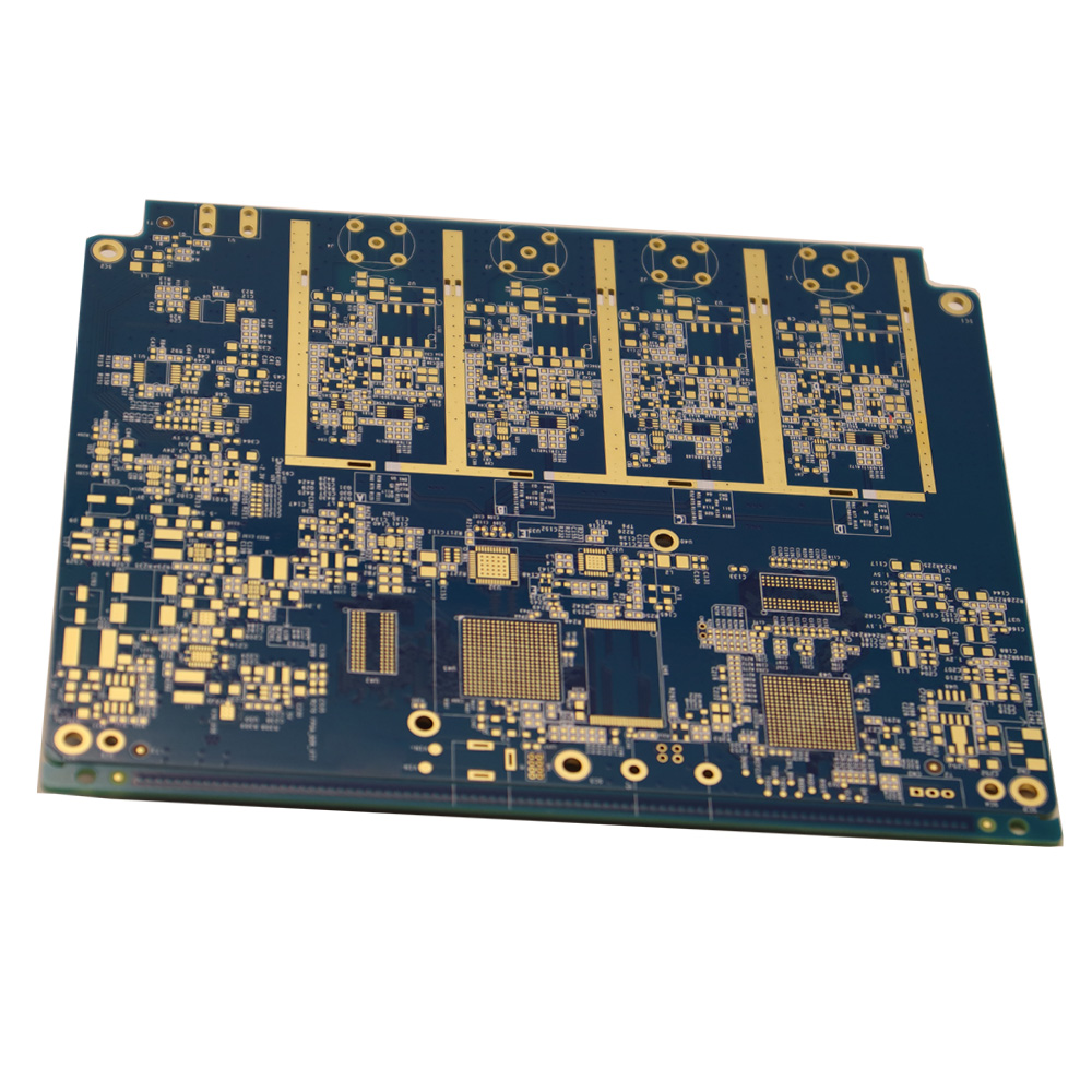
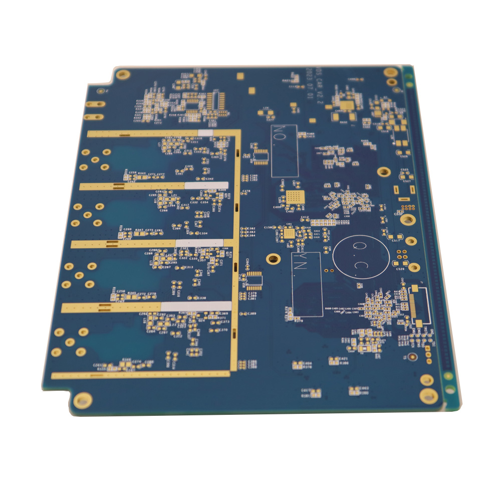
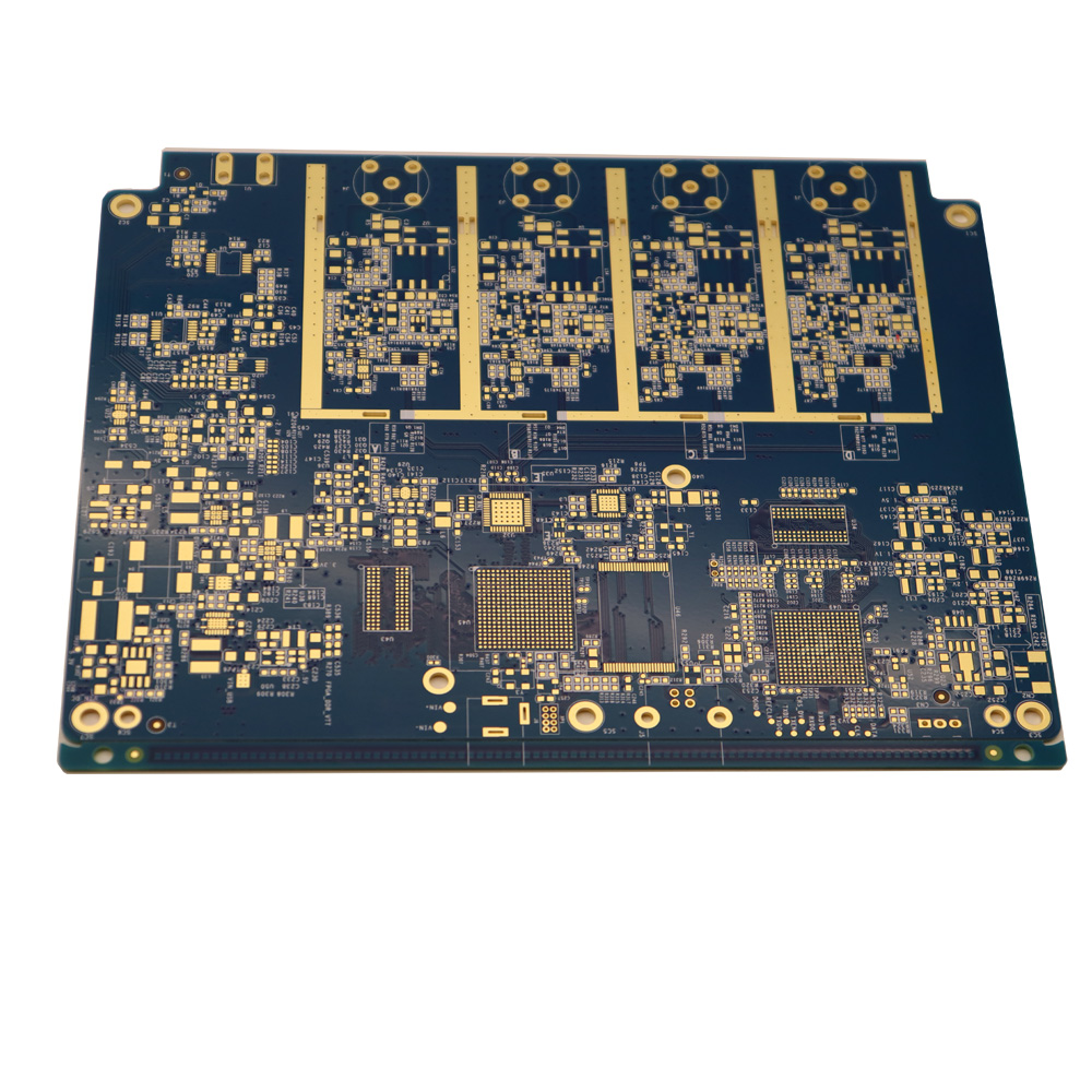
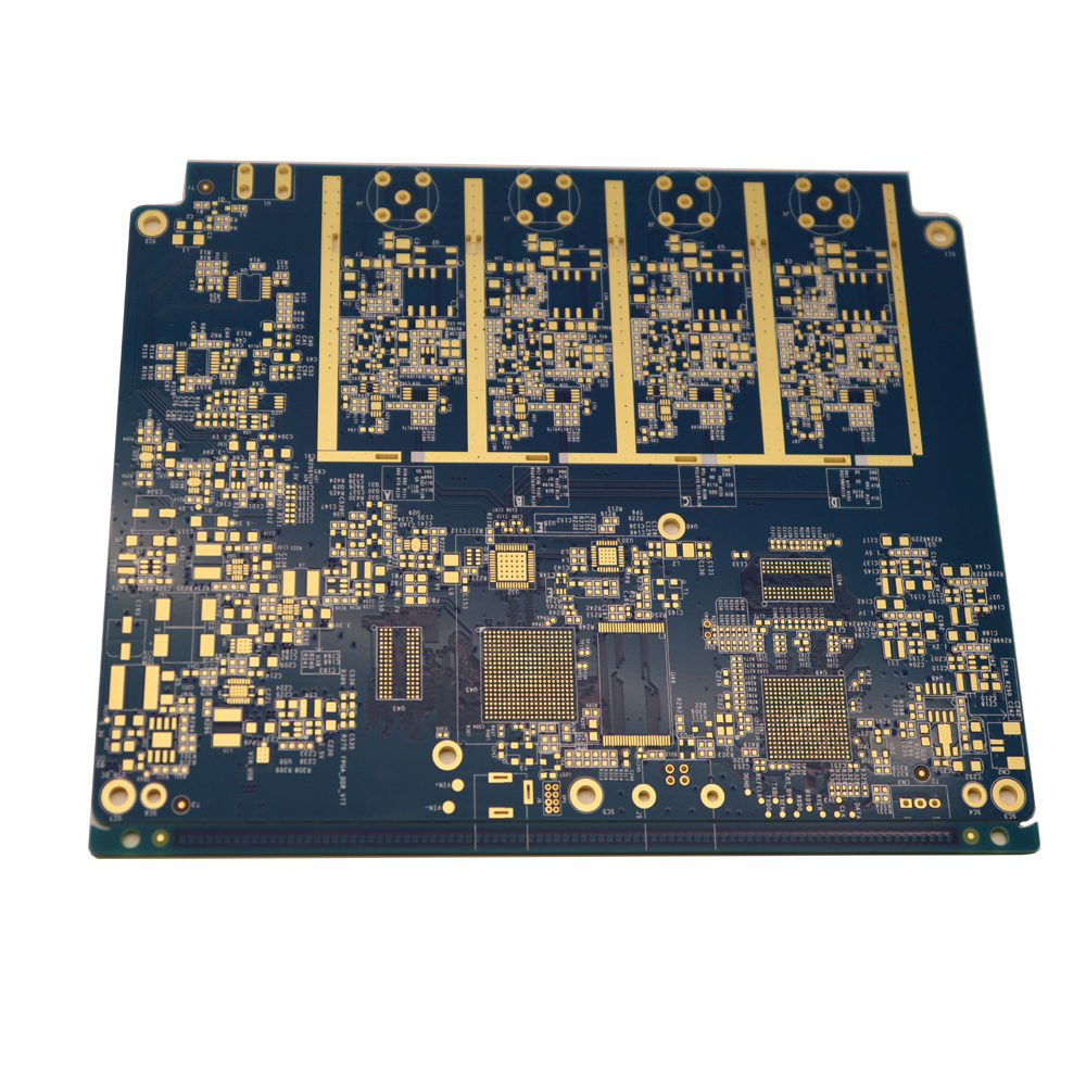
Part number:6G56073A0
PCB Layer:6 L
Material: FR4 Tg150 1.6mm 1oz finshed for all layer
Product flammability Rating: 94v0
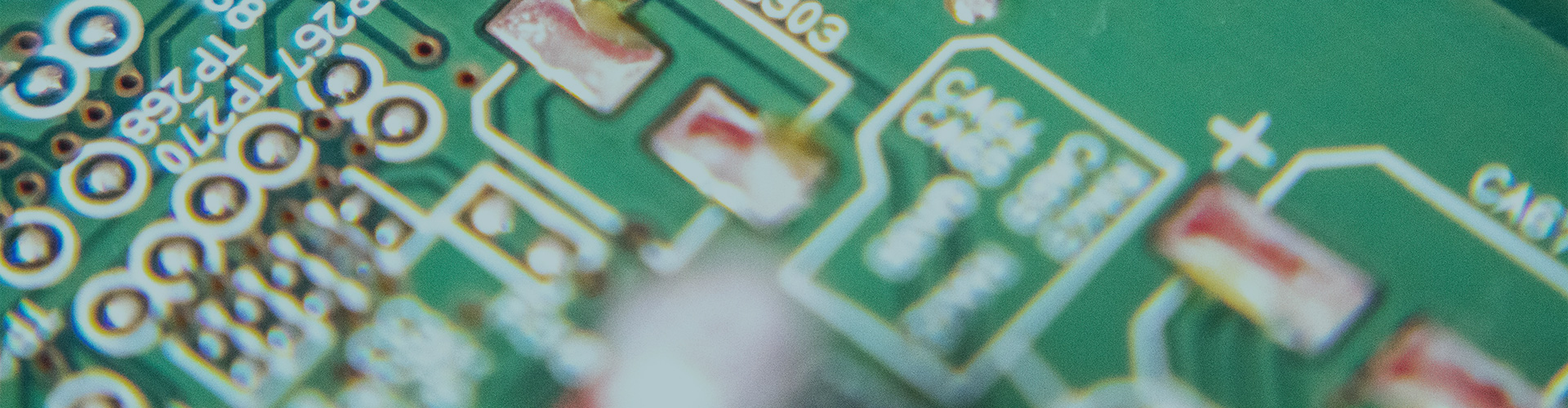
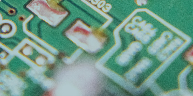
Product Type: Plating Through Hole PCB
PCB Style:Muiltilayer
Surface Finished:ENIG
Conductor width: 0.11mm
Conductor space:0.12mm
Min Hole size:0.20mm
Key Feature Description:
1) Impedance:50ohm,80ohm
2) Via hole :plugging
3) Solder ask:Blue LPI
4) BGA size:0.20mm
PCB manufacture flow:
This is the fabrication flow about the multilayer pcb board for plated through-hole PCB style, as you know,PCB of manufacture flows are too many, with more than 20 different processes, and each process has its sub-steps, Here, we will focus on the main manufacturing processes for reference
Process:

Why are there many high density design of PCB nowadays
High-density circuit design in PCB boards refers to the practice of placing a large number of electronic components and interconnections within a compact area. This approach is often used in advanced electronics, where space is limited, and performance requirements are high. The key benefits of high-density PCB design include:
Compact Size: High-density designs allow for smaller PCBs, making them ideal for compact devices like smartphones, tablets, and other portable electronics.
Improved Performance: With shorter signal paths, high-density designs can lead to faster signal transmission and reduced signal loss, enhancing the overall performance of the device.
Increased Functionality: High-density PCB designs can accommodate more features and functions on a single board, allowing for more complex and capable devices.
Cost Efficiency: By optimizing the use of space and materials, high-density PCBs can reduce the overall cost of production, particularly in large-scale manufacturing.
Enhanced Reliability: High-density designs often require more advanced manufacturing techniques, which can result in better-quality boards with fewer defects and higher reliability.
Technical Difficulty Control
 | 01 High precision Telecommunication Circuit Board High-density PCBs indeed pose significant challenges due to their smaller trace widths and spacing, and densely packed BGAs with small sizes. To successfully manufacture these boards, PCB manufacturers who must have advanced techniques, such as precise etching technology and cutting-edge exposure equipment etc. Without these, the pass rate can be severely impacted, leading to increased costs and production delays. Mastery in these areas is essential for maintaining high-quality production standards in high-density PCB manufacturing |
 | 02 Good Quality Made Good PCB quality stems from our company's commitment to technological innovation and relentless in-depth research. It is also a result of our advanced manufacturing equipment and the hard work of our well-trained, high-quality employees. Manufacturing such high-precision PCBs is challenging but achievable with the right technology and expertise. Dickson Circuits Shenzhen Ltd is proud to be a long-established professional PCB manufacturer with extensive experience in producing high-density PCBs, including HDI PCBs. Our strong process technology and advanced equipment ensure that our high-density multi-layer PCBs maintain stable quality, earning the trust and satisfaction of our customers. |
03 Manufacturer Description:
 | 1. Brand: SDY&Dickson 2. Company Certification: ISO9001,IATF16949,ISO140001 3.UL Recognized: USA UL, Canada UL,CQC 4. Product Manufacture Standard: refer to IPC standards •IPC-2222: Design standard. •IPC-4101: Laminate’s specification. •IPC-SM-840: Solder Mask Performance of Specification. •IPC-600: Rigid PCB Quality Inspection Standard. •IPC-6012:Rigid PCB Fabrication Specification. •IPC-6013:FPCB Fabrication Specification. •IPC-TM-650: PCB Quality Test Method. 5.Manufacture Service: Production Volume: 1) High-mix (Small,Medium and Large scale) 2) PCB Prototype:Yes 3) Quick-Turn PCB:Yes 4) Solder Paste Stencil Manufacturing |

Tel.: +86 0755 2332 1191
Fax: +86 0755 8176 4499
Add.: Building A1, Zone B, Ditang Industrial Zone, Shasan Community Agricultural Company, Shajing Street, Bao'an District, Shenzhen
Copyright © DICKSON Circuit Shenzhen Co., Ltd. All Rights Reserved | Technical Support: Nbone


 sales@dspcb.com
 +86 13828761409
 CN
CN Home >